First of all, I bought a cheap DEV board, that does not come with any kind of manual (not even a link to download it form the web), but I guess if you need a manual then you should leave these boards alone.
It features a Cyclone IV E, a cheap 622C8N, what else do you need to know, after all? :)
Ok, I tried/studied/experimented with a funny pong game that outputs to a VGA monitor.
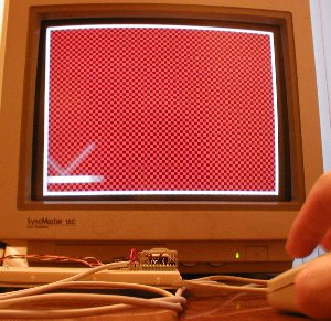
I did not connect it to the monitor yet, did not have time to solder a connector, but managed to probe the HSync and VSync signals with my DSO and they are as expected.
So I have been experimenting a bit with little verilog modules in Quartus II etc.
A funny thing I noticed is that each time I power cycled the board (or pressed the reset button), it would revert to the test program that was loaded when I received the board.
It is a bit weird if you come from the MCU world, but if you think it does make sense : FPGAs store their configuration in RAM, meaning that each time you reset them, they are completely blank, you need to pump in the configuration from a serial eeprom.
So, I figured out that each time I was writing the configuration to the RAM and not the eeprom itself, maybe there was some kind of option in the USB Blaster programmer...
Nope, not there, so I started checking the board schematics to see if I could locate the configuration device (the serial eeprom).

Sure enough I found a device in the JTAG section of the schematics that looked like a serial configuration storage, labeled EPCS4S18, which really looks like an Altera code related to Cyclone devices... a quick search on the web confirmed my first impressions.
Now, the interesting part is that my board comes with two programming sockets, with the same 10 pin JTAG standard connector , but only one is labeled JTAG, the other one, as visible in the schematics is labeled "AS".
Even more interesting is that the AS is connected to the EPCS4 device.

So, I figured that if the two ports had the same connector -probably- it was enough to connect the USB blaster on the AS one.
I left the quartus programmer on the JTAG option and obviously it gave me error, fair enough.
So I checked which other options were available and found an "Active Serial Programming" which kind of makes sense having a connector labeled AS, no?
Unfortunately as soon as I switched to Active Serial, a warning popped out telling me that I had no devices listed in the programming window that supported such mode.
The only device I had in my list was the Cyclone IV... but wait, I was actually trying to program the eeprom this time, not the fpga!
Clicked on "add device" (after accepting the Active Serial option which removed the FPGA device from the window) and there I found my beloved EPCS4!!
Now, I just needed to point to the binary file to be loaded... doh! The open file dialog filters for a different binary format called POF (instead of the common SOF used to program directly the FPGA chip).
Some more googling led me to this document which explains that serial configuration devices use Active Serial (which is supported by USB Blaster) to be programmed and they need this POF thing that is actually generated in Quartus II (File -> Convert Programming Files).

The process is quite straightforward :
1) Select your configuration device (EPCS4 in my case)
2) Click add File
3) Select the SOF file generated by the compiler
4) Click "Generate"
Then, in the programmer tool :

Make sure you connected your usb blaster to the AS port (if you have a board similar to mine), add the EPCS4 device, tag the program/configure option and finally "start".
The process is way slower than configuring the RAM, but it worked for me, and after resetting the board, the newly created configuration was active.
2 comments:
Hi
Thank you for this walk through for the FPGA begginers. I just have some questions.
1) So the connector labeled as "AS" is used just if I want my design to be permanently on the board?
2) With the connector labeled as "JTAG", am I able to download the hdl & nios to the fpga fabric and also debug the nios code? (understanding that everything will be lost if I remove the power to the board)
Yup, that's pretty much how I understood it too.
Checkign the schematics you can see that the AS is connected to the configuration device, while the JTAG goes striaght to the FPGA, basically sending data to it, bypassing the conf device.
When you cycle the power, if the JTAG is not connected, then the system will be configured from the conf devices, which you previously populated via the AS port.
Post a Comment